- 您现在的位置:买卖IC网 > Sheet目录342 > MCBSTM32EXL (Keil)BOARD EVALUATION FOR STM32F103ZE
�� �
�
�RM0008�
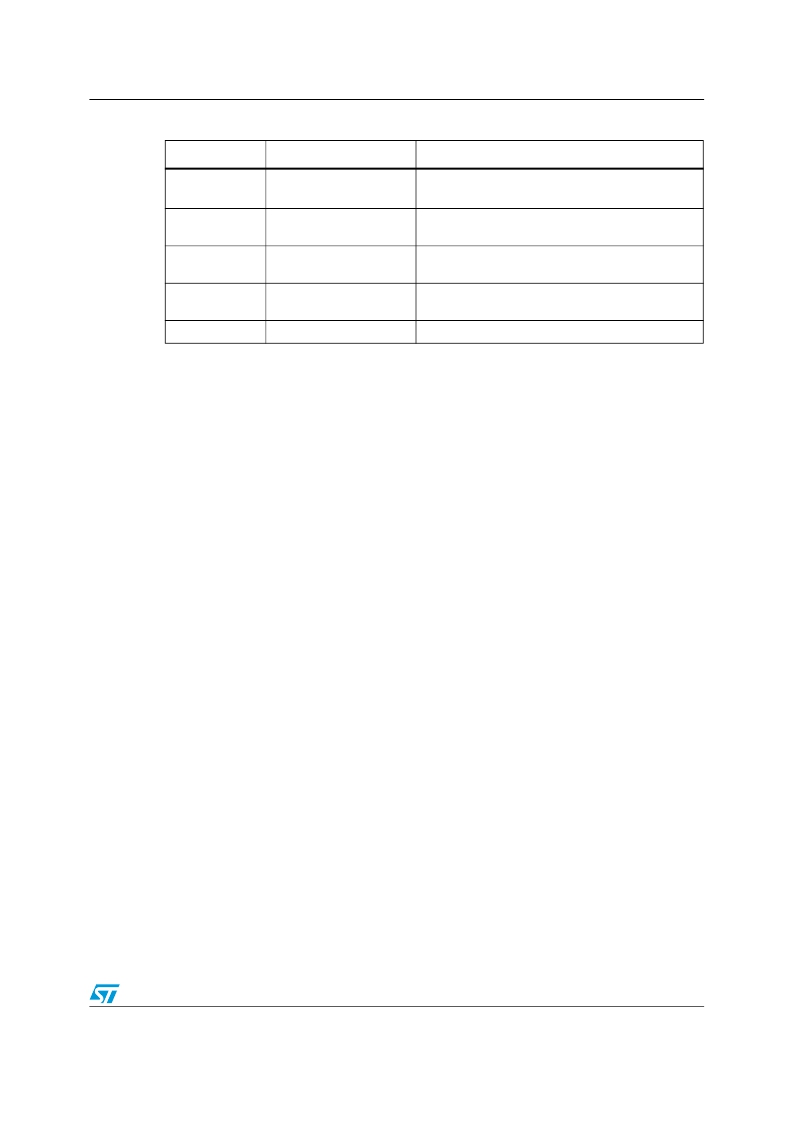
�Table� 60.�
�ADC� pins�
�Analog-to-digital� converter� (ADC)�
�Name�
�V� REF+�
�V� DDA�
�V� REF-�
�V� SSA�
�ADCx_IN[15:0]�
�Signal� type�
�Input,� analog� reference�
�positive�
�Input,� analog� supply�
�Input,� analog� reference�
�negative�
�Input,� analog� supply�
�ground�
�Analog� input� signals�
�Remarks�
�The� higher/positive� reference� voltage� for� the� ADC,�
�2.4� V� ?� V� REF+� ?� V� DDA�
�Analog� power� supply� equal� to� V� DD� and�
�2.4� V� ??� V� DDA� ??� V� DD� (3.6� V)�
�The� lower/negative� reference� voltage� for� the� ADC,�
�V� REF-� =� V� SSA�
�Ground� for� analog� power� supply� equal� to� V� SS�
�16� analog� input� channels�
�11.3.1�
�11.3.2�
�11.3.3�
�ADC� on-off� control�
�The� ADC� can� be� powered-on� by� setting� the� ADON� bit� in� the� ADC_CR2� register.� When� the�
�ADON� bit� is� set� for� the� first� time,� it� wakes� up� the� ADC� from� Power� Down� mode.�
�Conversion� starts� when� ADON� bit� is� set� for� a� second� time� by� software� after� ADC� power-up�
�time� (t� STAB� ).�
�You� can� stop� conversion� and� put� the� ADC� in� power� down� mode� by� resetting� the� ADON� bit.� In�
�this� mode� the� ADC� consumes� almost� no� power� (only� a� few� μA).�
�ADC� clock�
�The� ADCCLK� clock� provided� by� the� Clock� Controller� is� synchronous� with� the� PCLK2� (APB2�
�clock).� The� RCC� controller� has� a� dedicated� programmable� prescaler� for� the� ADC� clock,� refer�
�to� Low-,� medium-� and� high-density� reset� and� clock� control� (RCC)� on� page� 74� for� more�
�details.�
�Channel� selection�
�There� are� 16� multiplexed� channels.� It� is� possible� to� organize� the� conversions� in� two� groups:�
�regular� and� injected.� A� group� consists� of� a� sequence� of� conversions� which� can� be� done� on�
�any� channel� and� in� any� order.� For� instance,� it� is� possible� to� do� the� conversion� in� the�
�following� order:� Ch3,� Ch8,� Ch2,� Ch2,� Ch0,� Ch2,� Ch2,� Ch15.�
�●�
�●�
�The� regular� group� is� composed� of� up� to� 16� conversions.� The� regular� channels� and�
�their� order� in� the� conversion� sequence� must� be� selected� in� the� ADC_SQRx� registers.�
�The� total� number� of� conversions� in� the� regular� group� must� be� written� in� the� L[3:0]� bits� in�
�the� ADC_SQR1� register.�
�The� injected� group� is� composed� of� up� to� 4� conversions.� The� injected� channels� and�
�their� order� in� the� conversion� sequence� must� be� selected� in� the� ADC_JSQR� register.�
�The� total� number� of� conversions� in� the� injected� group� must� be� written� in� the� L[1:0]� bits�
�in� the� ADC_JSQR� register.�
�If� the� ADC_SQRx� or� ADC_JSQR� registers� are� modified� during� a� conversion,� the� current�
�conversion� is� reset� and� a� new� start� pulse� is� sent� to� the� ADC� to� convert� the� new� chosen�
�group.�
�Doc� ID� 13902� Rev� 9�
�201/995�
�发布紧急采购,3分钟左右您将得到回复。
相关PDF资料
MCBTMPM330
BOARD EVAL TOSHIBA TMPM330 SER
MCIMX25WPDKJ
KIT DEVELOPMENT WINCE IMX25
MCIMX53-START-R
KIT DEVELOPMENT I.MX53
MCM69C432TQ20
IC CAM 1MB 50MHZ 100LQFP
MCP1401T-E/OT
IC MOSFET DRVR INV 500MA SOT23-5
MCP1403T-E/MF
IC MOSFET DRIVER 4.5A DUAL 8DFN
MCP1406-E/SN
IC MOSFET DVR 6A 8SOIC
MCP14628T-E/MF
IC MOSFET DVR 2A SYNC BUCK 8-DFN
相关代理商/技术参数
MCBSTM32EXLU
功能描述:开发板和工具包 - ARM EVAL BOARD + ULINK2 FOR STM32F103ZG
RoHS:否 制造商:Arduino 产品:Development Boards 工具用于评估:ATSAM3X8EA-AU 核心:ARM Cortex M3 接口类型:DAC, ICSP, JTAG, UART, USB 工作电源电压:3.3 V
MCBSTM32EXLU-ED
制造商:ARM Ltd 功能描述:KEIL STM STM32EXL EVAL BOARD
MCBSTM32EXLUME
功能描述:开发板和工具包 - ARM EVAL BOARD + ULINKME FOR STM32F103ZG
RoHS:否 制造商:Arduino 产品:Development Boards 工具用于评估:ATSAM3X8EA-AU 核心:ARM Cortex M3 接口类型:DAC, ICSP, JTAG, UART, USB 工作电源电压:3.3 V
MCBSTM32F200
功能描述:开发板和工具包 - ARM EVAL BOARD FOR STM STM32F207IG
RoHS:否 制造商:Arduino 产品:Development Boards 工具用于评估:ATSAM3X8EA-AU 核心:ARM Cortex M3 接口类型:DAC, ICSP, JTAG, UART, USB 工作电源电压:3.3 V
MCBSTM32F200U
功能描述:开发板和工具包 - ARM EVAL BOARD FOR STM STM32F207IG + ULINK2
RoHS:否 制造商:Arduino 产品:Development Boards 工具用于评估:ATSAM3X8EA-AU 核心:ARM Cortex M3 接口类型:DAC, ICSP, JTAG, UART, USB 工作电源电压:3.3 V
MCBSTM32F200UME
功能描述:开发板和工具包 - ARM EVAL BOARD FOR STM STM32F207IG ULINK-ME
RoHS:否 制造商:Arduino 产品:Development Boards 工具用于评估:ATSAM3X8EA-AU 核心:ARM Cortex M3 接口类型:DAC, ICSP, JTAG, UART, USB 工作电源电压:3.3 V
MCBSTM32F200UME-ED
制造商:ARM Ltd 功能描述:KEIL STM32F207IG EVAL BOARD
MCBSTM32F400
功能描述:开发板和工具包 - ARM EVAL BOARD FOR STM STM32F407IG
RoHS:否 制造商:Arduino 产品:Development Boards 工具用于评估:ATSAM3X8EA-AU 核心:ARM Cortex M3 接口类型:DAC, ICSP, JTAG, UART, USB 工作电源电压:3.3 V